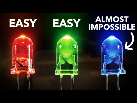
The Missing Spectrum: Why Blue Light Was the Holy Grail of Technology

For nearly thirty years, the world of electronics was stuck in a two-color era. After Nick Holonyak Jr. created the first visible red LED in 1962, followed shortly by green variants, the technological progress hit a wall. To create white light, which is essential for general illumination, scientists needed the third primary color: blue. Without it, LEDs were relegated to simple indicator lights on calculators and dashboards, unable to revolutionize the massive global lighting market.
Every major electronics giant, from IBM and GE to Bell Labs, poured millions of dollars and thousands of researchers into the hunt for the blue LED. They knew the prize was worth billions, yet by the late 1980s, most had given up. The physics required a large band gap material that could emit high-energy blue photons, a feat that seemed impossible under the manufacturing constraints of the time.
At a small chemical company called Nichia in Tokushima, Japan, a researcher named Shuji Nakamura was working in relative isolation. While the rest of the industry favored zinc selenide, Nakamura made the radical decision to focus on gallium nitride (GaN), a material widely regarded as a 'dead end.' His choice was driven by a desire to avoid the crowded field of competitors and carve out a unique path to a doctorate.
| LED Color | Material Era | Use Case |
|---|---|---|
| Red | Gallium Arsenide | Indicators, Displays |
| Green | Gallium Phosphide | Early Electronics |
| Blue | Gallium Nitride | Everything Modern |
Nakamura's early environment at Nichia was far from ideal. He worked with scavenged machinery and faced skepticism from his colleagues. However, this grit eventually led him to propose a 'moonshot' project to the company's founder, Nobuo Ogawa, who granted him $3 million—a massive gamble for a small firm—to chase the impossible blue light.
The Engineering Miracle: Building the Two-Flow MOCVD
Before Nakamura could tackle the light itself, he had to master the art of growing crystals. The industry standard was a process called Metal Organic Chemical Vapor Deposition (MOCVD), which works like a high-tech oven to layer atoms onto a substrate. Nakamura spent a year in Florida learning the basics, but he returned to Japan frustrated by his lack of academic recognition and the limitations of existing hardware.
Instead of following established protocols, Nakamura decided to take his reactor apart. He spent eighteen months in a relentless cycle of welding, cutting, and testing his machinery. He arrived at 7:00 AM every day, ignoring holidays and weekends, to perfect a new design he called the Two-Flow MOCVD. This invention used a secondary downward stream of gas to pin the reactant gases to the substrate, preventing turbulence.
ここからが大事な
ポイントです
具体例・注意点・明日から使えるヒントを整理しています。
✨無料閲覧で全文 + 図解の完全版を3日間いつでも読み返せる
あなたの好きな動画も、
1分でAI要約
📚 お気に入り保存 + ✨ あなたの動画をAI要約
(無料登録10秒)
✏️ この記事で学べること
- ▸LED
- ▸p
10秒で完了・パスワード作成不要